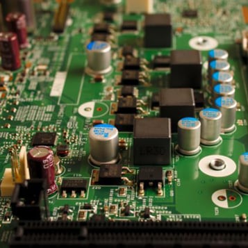
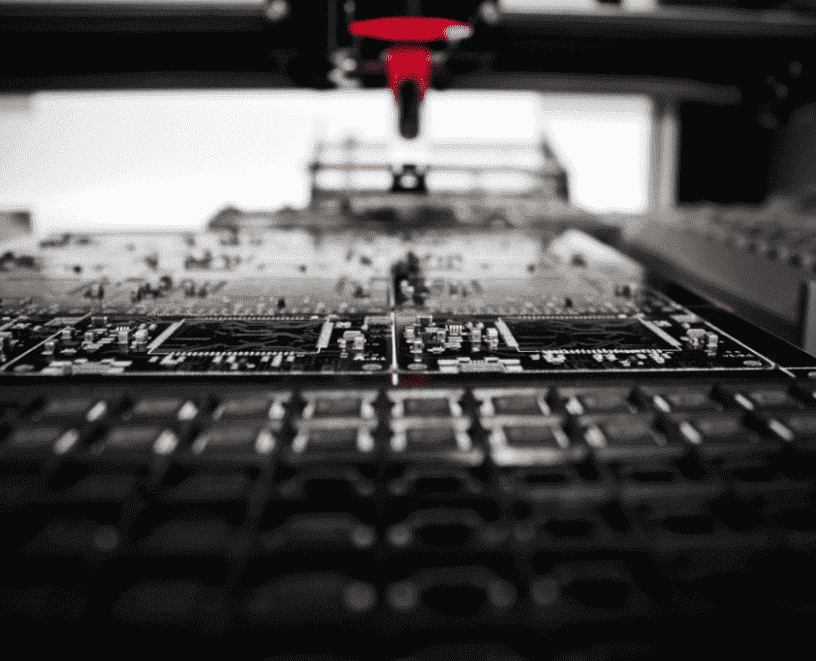
The 9 stages of printed circuit board production
Printed circuit board production is pretty straightforward for our customers.
From the moment you pick up the phone to us or drop us a message, we’ll walk you through everything we need for you to be able to deliver your printed circuit boards quickly and cost-effectively.
However, in case you ever wondered exactly what happens form start to finish of the printed circuit board production process, once you’ve made that initial contact, here’s the process from start to finish.
The printed circuit board production process is a lengthy one, and each element of the process is essential to ensuring your PCB is reliable and robust.
1. Front end engineering
First up, our team of skilled technicians review the Gerber files to check for any likely shorts or opens, or any ways that we can save you money or improve the effectiveness of your design. Many PCB manufacturers don’t offer this service, but we see it as part of our responsibility as your PCB production partner.
Then, using Genesis software with NC, AOI and test data, we create the tooling and plot files before sending them to the Silver Writer to laser plot the photo tools.
2. Drilling reference and tooling holes
Next up is to drill the reference and tooling holes.
These holes are essential as they help to ensure multiple layers are aligned, and also to line these layers up with stencils for solder paste printing and pick and place machines.
Our drilling department has 20 drilling spindles and 8 profiling spindles, all operated by Sieb & Meyer software controllers. The drills range from 2 to 6 spindle machines – ample capacity for low, medium and higher volume orders.
3. Preparing for copper plating
The next part of the process takes place in the wet shop where we apply a horizontal direct metallisation line which creates a conductive carbon layer in the hole of the PCB. We use an 8-cell copper plating line with pulse engines, and side-to-side rectification for enhanced accuracy.
4. Copper plating
Once the boards have been prepared for copper plating, they undergo plating. This involves submerging the boards into a copper plating solution where a layer of copper is deposited onto the conductive carbon layer created in the previous step. This copper plating step ensures that the conductive paths on the PCB are properly formed and ensures electrical connectivity throughout the board.
5. Outer layer imaging
After the copper plating, the outer layers of the PCB are imaged using a process called photolithography. In this step, a UV-sensitive photoresist material is applied to the copper surface, and then a mask containing the circuit pattern is placed over the board. The board is exposed to UV light, which causes the photoresist to harden in the areas not covered by the mask. The unhardened photoresist is then cleaned, leaving behind the circuit pattern on the copper surface.
6. Etching
Following the imaging step, the boards undergo etching to remove the excess copper from the surface. The areas of copper not protected by the hardened photoresist are dissolved away, leaving behind only the copper traces that make up the circuit pattern.
7. Solder mask application
Once the circuit pattern has been defined, a solder mask layer is applied to the board's surface. The particular solder mask is a protective layer that helps to insulate the copper traces and prevent them from oxidising. It also provides a smooth surface for soldering components onto the board.
8. Surface finish
After applying the solder mask, the boards undergo surface finishing to improve their durability and solderability. This involves applying a metal layer such as gold or tin to the exposed copper surfaces or hot air solder levelling (HASL), where the entire board is coated in solder and then levelled off to create a flat surface.
9. Electrical testing and inspection
The final stage of the PCB production process involves electrical testing and inspection to ensure that the boards meet the required specifications. This includes using automated testing equipment to check for continuity and shorts and a visual inspection to check for any defects or irregularities on the boards.
In conclusion, producing printed circuit boards involves a series of complex steps, each essential to ensuring the quality and trustworthiness of the outcome. From front-end engineering to electrical testing and inspection, every stage of the process requires precision and attention to detail to ensure that the finished boards meet the needs of our customers. By following these nine production stages, we can deliver high-quality PCBs quickly and cost-effectively, helping our customers bring their electronic designs to life.