PCB assembly: ball grid array explained
In our latest blog post, we consider the essential role of surface mount technology in printed circuit board assembly, along with the increasing use of ball grid array placement. Read on to learn more about how it works, the pros and cons, and tips for success.
What’s on this page
- What is ball grid array soldering?
- The advantages and disadvantages of ball grid array assembly
- PCB assembly: tips for success
What is ball grid array soldering?
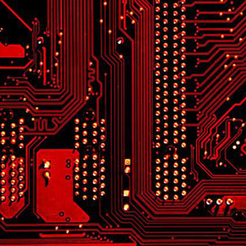
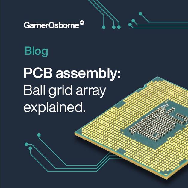
Ball grid array, or BGA, is one of the main package types for surface mount integrated circuits. First introduced in the 1990s, BGA was developed to overcome the issues posed by conventional pin grid array (PGA). In PGA integrated circuits, a high number of pins were positioned very close together. Unsurprisingly, this made soldering particularly challenging and increased the risk of the soldering joins and bridges collapsing.
Although derived from PGA, B[SP1] GA technology uses solder balls rather than pins to connect the components. As the name suggests, the solder balls are arranged in a grid pattern on the underside of the package (as opposed to the edges). The balls are positioned evenly apart, thereby reducing the chance of them accidentally bridging together. What’s more, because the leads in BGA packages are shorter than normal PCBs, they tend to deliver a better performance and higher speeds.
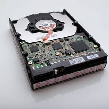
Ball grid assembly is typically used to permanently mount components in devices such as microprocessors.
The advantages and disadvantages of BGA assembly
Like any type of PCB assembly technique, a ball grid array package has its pros and cons. Rest assured, however, that our in-house experts are always on hand to talk you through the options and find the best PCB assembly solution for your needs.
Pros
- Facilitates high-density connections – BGA provides more connections than other types of surface mount packages, resulting in an improved design and performance
- High speed – as the solder balls are close together, there’s less chance of the signal being distorted during high-speed work. This means BGA packages provide excellent electrical performance
- Better thermal dissipation – BGA effectively dissipates the heat produced by the integrated circuit, thereby reducing the risk of the PCB overheating
- Excellent reliability – the pins used in PGA packages are quite fragile, which means they can be damaged relatively easily. Ball grid array packages, however, tend to be more reliable because the solder pads are connected to the solder balls.
Cons
- Difficult to inspect – due to their small size, visually inspecting the solder joints can be difficult. Special microscopes and x-ray machines have therefore been developed to help overcome this challenge
- Cost of equipment – the equipment required for BGA soldering is expensive, although most experts tend to agree that the overall benefits of BGA packages compensate for the higher upfront cost.
If you’d like to find out more about the different PCB assembly methods, get in touch with our friendly team today.
PCB assembly: tips for success
- Ensure components are spaced appropriately
It’s important not to place integrated circuits too close together. The exact distance depends on various factors, but it’s good practice to allow several millimetres between each component. You should also avoid placing components too close to the edge of the PCB.
- Design for easy inspection
When planning the layout of a PCB, it’s a good idea to design the placement of components in a way that makes them easy to inspect, fix and maintain. Of course, this isn’t always possible but it’s certainly worth bearing in mind – you’ll thank yourself later!
- Ensure the footprint matches the datasheet
The footprint plays an essential role in the assembly process as it allows PCB manufacturers to determine exactly where the components need to sit on the board. To help ensure the manufacturing process runs as smoothly as possible, it’s good practice to check the footprint matches the datasheet.
- Opt for single-sided SMT wherever possible
If you’re keen to keep manufacturing costs down, consider opting for a single-sided printed circuit board. Not only does its simpler design make it highly affordable, but it also minimises the risk of potential problems and speeds up production times. You can read more about the different types of PCBs here.